GHz quantum circuits
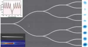
We demonstrate 2D, continuous variable (CV) cluster states between ~102 modes of a microwave frequency comb, obtained by injecting vacuum fluctuations thermalized at 10 mK into a Josephson Parametric Amplifier pumped by a sum of coherent signals around double the center-comb frequency. This enables frequency mixing and two-mode squeezing between different frequency modes. By carefully tuning pump frequencies, amplitudes, and phases we engineer interference between mixing products and realize square-ladder, honeycomb and square lattice CV cluster states with three and four pump tones, respectively. We prove the presence of a cluster state and reach up to 1 dB of squeezing of the cluster state’s nullifiers.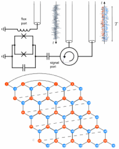
Lingua, et al., Continuous-variable square-ladder cluster states in a microwave frequency comb, PRL 134, 18362 (2025)
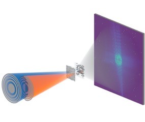
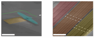
Multi-beam multi-slice 3D X-ray ptychography
We demonstrate the first integration of multi-beam ptychography with multi-slice reconstruction, enabling high-resolution 3D imaging of nanostructures within thick samples. By combining the efficiency of parallelized multi-beam acquisition with the ability of multi-slicing to model multiple scattering events, we overcome the resolution limitations that have restricted conventional large-volume ptychography. Our approach yields isotropic resolution at depths comparable to the lateral dimensions accessible with state-of-the-art multi-beam setups. The method is robust, reproducible across synchrotron beamlines, and directly applicable to a wide range of scientific problems requiring non-destructive 3D imaging of extended samples — a new foundation for efficient, high-resolution X-ray microscopy of complex materials and devices.
Åstrand, et al., Multi-beam multi-slice X-ray ptychography, Scientific Reports 15, 9273 (2025)
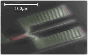
Quantum many-body effects in CMOS-compatible photonic IC’s
We provide the first experimental evidence of multiple mobility edges in quasiperiodic mosaic lattices using integrated CMOS-compatible photonic circuits. By engineering site-dependent quasiperiodic potentials and probing single-site excitations, we directly observe the coexistence of localized and extended states in the same lattice. This demonstrates the breakdown of self-duality symmetry and validates recent theoretical predictions from Avila’s global theory. Our results mark a significant step in exploring energy-dependent localization transitions and open avenues for investigating quantum many-body effects with hybrid integrated photonic devices.
Gao, et al., Probing multi-mobility edges in quasiperiodic mosaic lattices, Science Bulletin 70, 58 (2025)
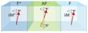
Nonlinear magnonics
A hybrid material of alternating thin ferromagnetic and antiferromagnetic (AF) layers is found to exhibit a highly nonlinear microwave response, which is strongly dependent on temperature near in the Neel point of AF. The relative nonlinearity approaches 100%, which is much larger compared, for example, to popular optical nonlinear materials generating second harmonics at single percentage levels. The material properties demonstrated are interesting for thermo-magnonic applications, where additional functionality can be achieved using thermal control in a narrow range near room temperature.
Busel, et al., Nonlinear spin dynamics across Néel phase transition in F/AF multilayers, APL Materials 13, 071121 (2025)
Generation of twin photons in nonlinear nanostructures
Spontaneous parametric down-conversion (SPDC) enables the generation of polarization- and spectral-indistinguishable photons, important for quantum photonic circuits. We demonstrate the generation of counterpropagating twin-photon pairs in the optical communication band using periodically poled Rb-doped KTiOPO4. At degeneracy, the photon pairs exhibit a broad angular distribution, where the forward-propagating photon tunes with the pump frequency while the backward-propagating photon frequency is nearly independent of the pump wavelength.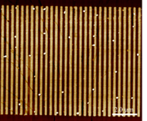
Amores, et al., Generation of counterpropagating photon pairs in periodically poled Rb-KTiOPO4, Phys. Rev. A 112 , 032608 (2025)
Acoustic modulation of Q-dots for entangled-photons generation
We demonstrate acoustic modulation of individual nanowire quantum dots (QDs) integrated into a hybrid thin-film lithium niobate platform with silicon nitride-loaded waveguides. By driving surface acoustic waves at 400 MHz, we achieve wavelength modulation up to 1.4 nm and bring two distinct QDs into spectral overlap on the same chip. This local strain-tuning method enables synchronization of remote emitters, a critical step toward generating indistinguishable single photons for scalable quantum photonic circuits.
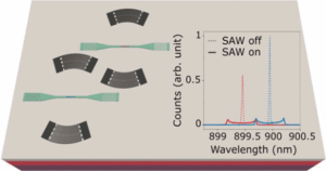
Descamps, et al., Acoustic Modulation of Individual Nanowire Quantum Dots Integrated into a Hybrid Thin-Film Lithium Niobate Photonic Platform, Nano Letters 24, 12493 (2024)
Single-photon detectors on LNO
We present the integration of wavelength-sensitive superconducting nanowire single-photon detectors (SNSPDs) directly onto thin-film lithium niobate waveguides. Leveraging the intrinsic dependence of SNSPD responsivity on photon energy, we demonstrate an on-chip wavelength meter operating across the telecom C- and L-bands. The detectors show low jitter, high internal efficiency, and a compact footprint of only 300 × 180 μm², paving the way for scalable wavelength-multiplexed quantum communication systems on lithium niobate photonic circuits.
Prencipe, et al., Wavelength-Sensitive Superconducting Single-Photon Detectors on Thin Film Lithium Niobate Waveguides, Nano Letters 23, 9748 (2023)
Superconducting vortex memory
We demonstrate vortex-based superconducting memory cells, test scalability and show that the cells can be miniaturized to submicron sizes. We introduce an asymmetric easy track for vortex motion and show that it enables a controllable manipulation of vortex states. Finally, we perform a detailed analysis of word and bit line operation of a 1 × 1 μm2 cell. High-endurance, non-volatile operation at zero magnetic field is demonstrated. Remarkably, we observe that the combined word and bit line threshold current is significantly reduced compared to the bare word-line operation. This could greatly improve the selectivity of individual cell addressing in a multi-cell RAM. The achieved one square micron area is an important milestone and a significant step forward towards creation of a dense cryogenic memory.
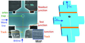
Golod, et al., Word and bit line operation of a
1 x1 μm2 superconducting vortex-based memory, Nature Commun. 14, 4926 (2023)
Entangled photons on-chip
We report the scalable generation and detection of on-demand W states in nanophotonic circuits, a key step toward robust multipartite quantum entanglement on-chip. Using single photons from nanowire quantum dots integrated with a CMOS-compatible silicon nitride photonic chip, we realize an eight-mode W state through cascaded Y-splitters. The entangled nature of the state is verified using real- and Fourier-space imaging combined with the Gerchberg–Saxton phase retrieval algorithm and entanglement witnesses. This approach introduces a reliable and scalable method to reconstruct and validate multipartite entangled states in integrated photonics, paving the way for high-rate quantum communication and information processing.
Gao, et al., Scalable Generation and Detection of on-Demand W States in Nanophotonic Circuits, Nano Letters 23, 5350 (2023)
..
Strain-modulated Q-dots
We demonstrate the dynamic strain modulation of a nanowire quantum dot integrated with a lithium niobate photonic platform. By coupling surface acoustic waves to the nanowire quantum dot, we achieved reversible tuning of the emission wavelength while preserving high single-photon purity. Importantly, the approach remains effective even with a SiO₂ encapsulation layer, which both stabilizes the nanowire and acts as a photonic cladding. Based on these findings, we propose a scalable device architecture combining strain-tunable quantum dot emitters with thin-film lithium niobate rib waveguides, opening pathways for reconfigurable quantum photonic circuits.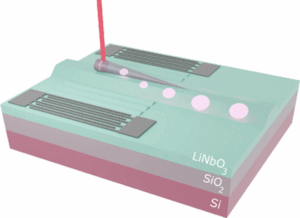
Descamps, et al., Dynamic Strain Modulation of a Nanowire Quantum Dot Compatible with a Thin-Film Lithium Niobate Photonic Platform, ACS Photonics 10, 3691 (2023)
High-resolution electron-beam lithography
We demonstrate a theory, correction method, and implementation to overcome dose insufficiency in electron-beam lithography (EBL) of thick resist layers at the nanoscale. By identifying the proximity effect as the origin of insufficient energy delivery to small features, we establish a proximity effect correction (PEC) algorithm that assigns the correct area dose during patterning. Applied to direct-write 50 kV EBL on AR-P 6200 (CSAR 62) resist, this approach enables fast, inexpensive exposures while maintaining compatibility with downstream processes. We achieve high-quality nanostructures at high aspect ratios, providing an accessible and robust route for precision nanofabrication.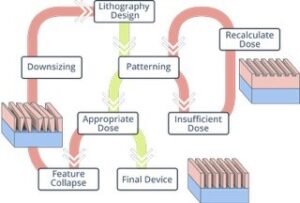
Åstrand, et al., Understanding dose correction for high-resolution 50 kV electron-beam lithography on thick resist layers, Micro and Nano Engineering 16, 100141 (2022)
Superconducting diodes
We demonstrate prototypes of superconducting diodes operational at zero magnetic field. They are based on conventional niobium planar Josephson junctions, in which space/time symmetry is broken by a combination of self-field effect from nonuniform bias and stray fields from a trapped Abrikosov vortex. We show that nonreciprocity of critical current in such diodes can reach an order of magnitude and rectification efficiency can exceed 70%. Furthermore, we can easily change the diode polarity and switch nonreciprocity on/off by changing the bias configuration and by trapping/removing of a vortex. This facilitates a memory functionality. We argue that such a diode-with-memory can be used for future generations of in-memory superconducting computers.
Golod, et al., Demonstration of a superconducting diode-with-memory, operational at zero magnetic field with switchable nonreciprocity, Nature Communications 13, 3658 (2022)
Nanomaterials for energy applications
The group led by Muhammet Toprak develops thermoelectric nanomaterials to harvest waste thermal energy in the surrounding and convert into electrical power. The group recently developed an ink/paint formulation using a combination of green-chemical synthesis, surface-interface engineering, and additive manufacturing strategies [1]. The developed paint can be coated on the surfaces generating heat, enabling locally generated heat that can be used to power some other tools. The group exploits the implementation of this paint concept for harvesting body-heat to power wearable electronics, sensors, and low-power applications in the internet of things (IoT).

Serrano-Claumarchirant, et al., Thermoelectric Inks and Power Factor Tunability in Hybrid Films through All Solution Process, ACS Appl. Mater. Interfaces, 14, 19295, (2022)
Press release on this milestone at KTH-web, and national/international news: KTH: nyheter, FORSKNING.SE, AZOM.COM, SWIPENEWS
CMOS compatible nanophotonics
Our team has demonstrated the direct measurement of topological invariants in photonic superlattices using a CMOS-compatible nanophotonic chip. By engineering chiral lattices with broken inversion symmetry and introducing nanoscale scattering structures, we developed a single-shot method to probe the light dynamics and directly extract quantized topological numbers. This approach allows clear identification of trivial and nontrivial topological phases, marking a significant step toward topologically robust multi-band photonic devices.
Xu, et al., Direct measurement of topological invariants in photonic superlattices, Photonics Research 10, 2901 (2022)
Integrated single-photon emitters
The promise of a quantum internet depends on the complexities of harnessing light to transmit quantum information over fiber optic networks. A potential step forward was reported today by researchers at KTH who developed integrated chips that can generate light particles on demand and without the need for extreme refrigeration.
Deterministic Integration of hBN Emitter in Silicon Nitride Photonic Waveguide
Elshaari, et al., Deterministic Integration of hBN Emitter in Silicon Nitride Photonic Waveguide, Advanced Quantum Technologies 4, 2100032 (2021)
Cover page Wiley Journal article, Chalmers WACQT News, KTH News, Qubit Report, Advanced Science News
Single-photonics on a Chip
In a potential boost for quantum computing and communication, our European research collaboration reports a new method of controlling single photons without generating heat. The solution makes it possible to integrate optical switches and single-photon detectors on a single chip. We have developed an optical switch reconfigurable by microscopic mechanical movement rather than heat, making the switch compatible with heat-sensitive single-photon detectors. Using microelectromechanical (MEMS) actuation, the device enables integrated optical switching and photon detection, at cold temperatures required by single-photon detectors.
Gyger, et al., Reconfigurable photonics with on-chip single-photon detectors, Nature Comm. 12, 1408 (2021). Coverage: KTH Press Release, European Commission, phys.org, EurekAlert.
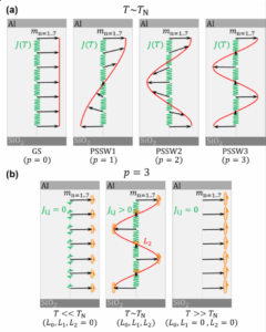
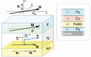
GHz Spintronics
We demonstrate strong thermally controlled magnon-mediated interlayer coupling of two ferromagnetic layers via an antiferromagnetic spacer in spin-valve trilayers. The effect manifests itself as coherent switching and collective resonant precession of the two ferromagnets, which can be controlled by varying temperature and the spacer thickness. We explain the observed behavior as due to a strong hybridization of the ferro- and AF magnon modes in the trilayer at temperatures just below the Neel temperature of the spacer. The observed spin-wave dynamics is highly non-linear and can be conveniently controlled by thermal gating the multilayer. The highly nonlinear material properties demonstrated are interesting for spin-thermionic and thermo-magnonic applications, where additional functionality
can be achieved using thermal control in a narrow range near room temperature.
Polishchuk, et al., Thermal Gating of Magnon Exchange in Magnetic Multilayers with AF Spacers, PRL 126, 227203 (2021)
High-power THz Generation
We have demonstrate multi-cycle terahertz (MC-THz) generation in periodically poled rubidium (Rb)-doped potassium titanyl phosphate (Rb:PPKTP) crystal. The maximum internal optical-to-terahertz conversion efficiency achieved is comparable with results achieved using periodically poled lithium niobate crystals. Neither photorefractive effects nor damage was observed with up to 1 J/cm^2, showing the great potential of Rb:PPKTP for multi-millijoule-level MC-THz generation.

Record high THz energy using Rb:KTP
Tian, et al., mJ-level multi-cycle terahertz generation in a periodically poled Rb:KTP crystal, Optics Letters 46, 741 (2021)
Intermodulation Products
KTH-ANL hosts the biggest and most versatile atomic force microscopy (AFM) lab in Sweden. Thanks to this rich and flexible environment, Intermodulation Products AB was founded as a spinoff of the Haviland group KTH. Intermodulation Products AB commercializes add-on equipment to labs and users who want to extend the measurement capabilities of their AFM with mechanical, electrical and magnetic characterization, for applications ranging from energy materials to life sciences. All the special modes developed by Intermodulation Products are available to users of ANL-AFMs. The start-up is actively expanding its products space, e.g. to high-speed multi-frequency lock-in systems.

Comparison of Intermodulation EFM and KPFM at ANL. Maps and histograms of work function in volts measured on graphene monolayer (blue) with flakes of bilayer graphene (yellow). Graphene is thermally grown on silicon carbide (SiC) substrate. White scale bars are 3 μm.
R. Borgani, PhD Thesis, KTH 2018.
Single Quantum
Single Quantum, a spinoff from the Zwiller group at KTH, commercializes high-performance single-photon detectors based on superconducting nanostructures. The outstanding superconducting film deposition and nano-patterning processes available at KTH-ANL enable joint R&D of KTH and Single Quantum on developing a new generation of single-photon detectors with the time resolution, noise level, and detection efficiencies setting new standards in quantum optics. The application space is quantum communications, where SQ is one of the leaders internationally.

Figure main panel: top view of superconducting NbTiN meander-patterned single-photon detector; top-left: meander-nanowire close-up; bottom-right: detector integrated with optics.
Zichi, et al., Optimizing the stoichiometry of ultrathin NbTiN films for high-performance superconducting nanowire single-photon detectors, Opt. Express 27, 26579 (2019)
Antiferromagnetic spintronics
We have demonstrated tunable relaxation of a pure spin current by an antiferromagnet in spin-valve type multilayers. This is achieved by carefully controlling the angle between a resonantly excited ferromagnetic layer at >10 GHz, pumping the spin current and the Neel vector of the antiferromagnetic layer. The effect is observed as an angle-dependent spin-pumping contribution to the ferromagnetic resonance linewidth. An interplay between spin-mixing conductance and, often disregarded, longitudinal spin conductance is found to underlie our observations, which is in agreement with a recent prediction for related ferromagnetic spin valves. These results contribute to scaling spintronics to sub-THz frequencies.
Polishchuk, et al., Angle Resolved Relaxation of Spin Currents by Antiferromagnets in Spin Valves, PRL 123, 247201 (2019)