ALD Atomfab PlasmaPro ASP for Q-Tech R&D by Oxford Instruments
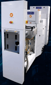
Plasma-enhanced atomic layer deposition system for high quality materials, such as Ti-N, Nb-N, Al-O, Hf-O, including ultra-thin quantum materials and multilayers, that can be deposited at speed, with flexibility to run multiple chemistries to give excellent layers for incorporation into devices:
- high material quality at 3x faster than conventional remote plasma
- reduced precursor consumption, small budget and environmental footprint
- low cost of ownership, improved serviceability and maintenance
- low volume chamber for speed
- low substrate damage
- higher process stability
Installation Fall 2025
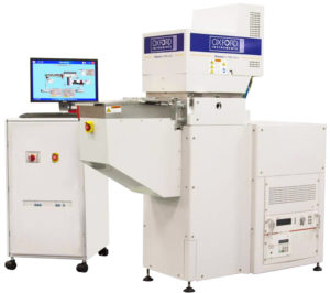
ICP-CVD PlasmaPRO 100 by Oxford Instruments
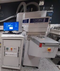
Chemical vapor deposition system for growing films at low temperature through high-density remote plasma, achieves superior film quality with low substrate damage: Si oxide, nitride, carbide, amorphous Si, variety of other materials possible (via addon modules). Features:
- excellent uniformity, high precision, high throughput
- wide temperature range electrode, capability from -150 to 400 C
- all wafer sizes up to 200 mm, rapid change between sizes
- in-situ chamber cleaning and end-point
- flexible vapor delivery module enables liquid precursors, e.g. TiO2, SiO2
In operation since May 2025
HV e-beam evaporating system by Kenosistec
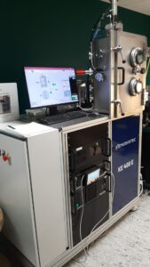
Versatile e-gun evaporator with:
- HV door-access chamber, turbo pump 1200 l/s
- base pressure < 2*10^-7 Torr, 1*10^-6 within 30 minutes
- e-gun with 4 pockets of 4 cc capacity, 350 mm source-substrate distance
- automatic indexing, programmable sweep parameters
- removable substrate plate for single 100mm wafer and small chips
- dome platen available for five 100 mm wafers
- relaxed requirements on materials/substrates compared to our UHV systems
In operation since March 2024
FIB-SEM Helios 5 UC, FEI-Thermo Fisher Scientific
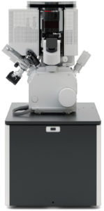
Dual beam FIB-SEM system with:
- electron source with monochromator technology
- energy spread of 0.2 eV for beam currents up to 100 pA
- SEM resolution 0.6 nm at 15 kV (landing energy 20 eV – 30 keV), 0.7 nm at 1 kV
- retractable STEM detector
- ion beam (Ga++) 1 pA – 100 nA, 500 V – 30 kV, resolution 4.0 nm at 30 kV
- Pt gas injection system
- fully software integrated micro manipulator
- piezo XY stage with XY repeatability of 1 µm
In operation since October 2023
DynaCool PPMS, Quantum Design
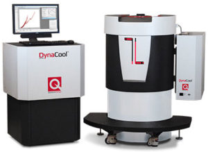
Physical Properties Measurement System, DynaCool, Quantum Design. Base system temperature range 2 to 400 K, electrical measurements (resistance, AC-resistance, I-V characteristics), magnetic measurements (VSM, AC-susceptibility), thermal measurements (heat capacity), RF-insert.
In operation since July 2022
ATC Orion Series Ion Milling System, AJA International
The ATC-Orion is a ion-milling system with a gridded filament ion source capable of 250 mA maximum beam current. Beam voltage 100 – 1200V, 200 mA beam current @1000V. Water cooled tilting and rotating substrate holder for up to four inch diameter substrates. Continuous motorized rotation (0 – 20 rpm), ferro-fluidic rotary seal allows +/- 90° tilting.
In operation since July 2023
PPMS EverCool II, Quantum Design
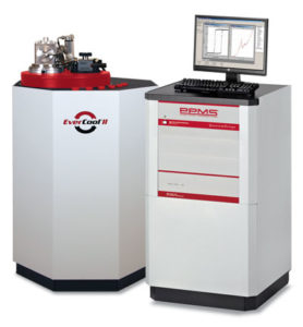
Magnetic, electrical, thermal, mechanical, optical measurements at low temperatures. Closed helium cycle. Material characterization at 1.9 – 400 K, superconductive 9 T magnet. Can be fitted with measurement options for magnetic moment, susceptibility, resistivity, Hall coefficient, thermal capacity, thermal expansion and more.
In operation since November 2022
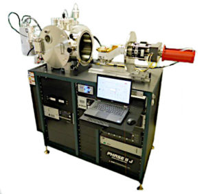
ATC-1800-HY UHV Multi-Technique Deposition System, AJA International
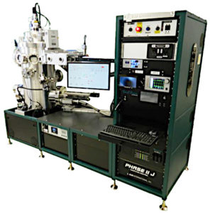
The ATC-1800-HY is a deposition system with in-situ crucible exchange system. This enables crucible exchange without breaking vacuum. The system comes with six 15 cc crucibles with automated indexing. E-beam source is a 6 kW High Voltage Supply with automated sweep control, no need for manually aiming the beam correctly in the crucible. Two magnetron sputtering sources using 3 inch targets. The sputtering sources have two generators, 1500 W DC and 600 W RF generator. Direct sputtering, working distance < 10 cm. Kaufman KDC 40/75 Ion Sources for milling / pre-cleaning. Water-cooled, rotating and tilting substrate holder for substrates up to 4 inch dia. Three gas-lines for Ar, O2 and N2. Multi-Wavelength Ellipsometer System, spectral range 405 – 950 nm. Possibility to do oxidation inside the load-lock.
In operation since July 2023
VASE Ellipsometer, J.A. Wollam
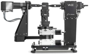
VASE Ellipsometer-Spectrometer measures the optical constants and thickness of films, multilayers or bulk materials, as well as the reflection/transmission as a function of angle of incidence (12° to 90°), polarization, and wavelength in the UV-IR range: 240 nm – 2500 nm, 4 um option available. Beam focusing option available for testing small structures.
In operation since May 2022
Plasma etcher PlasmaPro 100 Cobra 300 ICP, Oxford Instruments
The Oxford PlasmaPro 100 Cobra 300 is a load locked plasma etcher with a cryo stage. Maximum wafer size is 200 mm. Etch rate is > 8 um/min with a 3 kW ICP RF generator. Selectivity for photoresist is > 120 (general Bosch process).
In operation since April 2022
Photolithography tool MaskLess Aligner MLA 150, Heidelberg Instruments
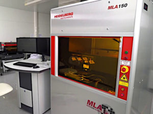
The MLA 150 (MaskLess Aligner) Direct Laser Writer is capable of photolithography of details down to 0.6 um (min. feature size). It uses a UV diode laser illumination of 375 nm for broadband and i-line photoresists, such as SU-8, AZ-nLOF, TOK IP and others. The option of Back Side Alignment (BSA) is included, thus adding the possibility of exposing backside of substrate. Maximum substrate size is 6 x 6 inches, minimum size is 5 x 5 mm (due to auto focus mechanism). Maximum write area is 150 x 150 mm, and substrate thickness can be between 0.1 to 12 mm.
In operation since June 2021
EDS detector AZtec, Oxford Instruments
Detector for Electron Dispersive Spectroscopy (EDS) is added to the Albanova Nanolab FIB/SEM, FEI Nova 200. This opens the possibility of material analysis using the scanning electron beam of the SEM as probe. It is possible to do “live” material analysis during scanning of SEM images, as well as color mapping of different materials as an overlay on the SEM image. Quantitative analysis of element content is also possible.
In operation since December 2019
Stylus Profilometer P – 7, KLA Tencor
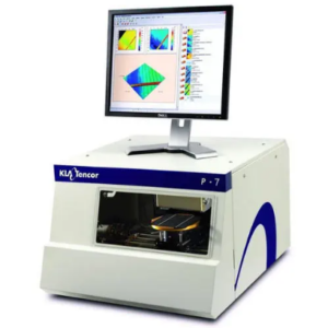
Stylus Profilometer P – 7. The system supports 2D and 3D measurements of step heights, roughness, bow, and stress for scans up to 150mm without stitching. Stylus radius 2 µm.
In operation since Spring 2020